
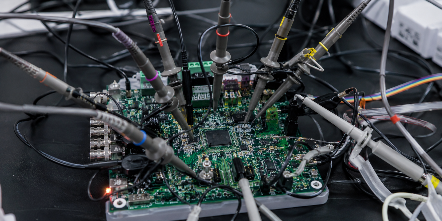
“Invasive” sounds like it means “we cut into the board.” In the classification that actually defines the term, it doesn’t.
The standard taxonomy in hardware security (non-invasive, semi-invasive, invasive) draws its line at the chip package, not at the PCB. What happens to the board around the chip is irrelevant to which category an attack falls into. That distinction matters, because it’s easy to assume “non-invasive” means “we didn’t touch anything,” and on real hardware that’s rarely true.
Non-invasive: the chip package stays sealed
By definition, non-invasive covers everything that doesn’t require opening the chip:
- Side-channel analysis: power consumption, electromagnetic emissions, timing
- External fault injection: voltage glitching, clock glitching, applied through the device’s existing pins or power rails
- Interface-level attacks: JTAG/SWD exploitation, protocol abuse, brute force through whatever I/O the device exposes
The category is defined by the chip, not by what it took to reach it. You can desolder a shield, tap a buried trace, or bridge a modified connection to get a glitch signal onto the right pin; the chip is still sealed, so the attack is still, technically, non-invasive.
Before the board: sealed enclosures and potting compounds
The taxonomy above assumes a bare board. A lot of real hardware doesn’t arrive that way. Industrial, Automotive and IoT devices are frequently potted (epoxy, polyurethane, or silicone resin poured over the assembly) for environmental protection, and just as often, deliberately, to make board-level access harder to get to.
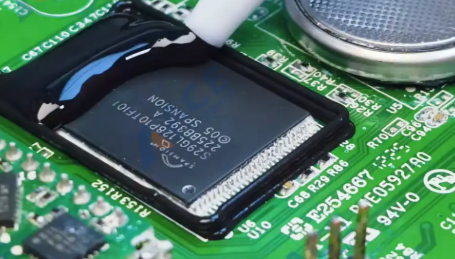
Getting to the PCBA is a phase of its own, and it happens before anything above applies:
- Resin identification first: epoxy, polyurethane, and silicone respond completely differently to heat and solvents, and treating one like another is how the PCB gets destroyed fast
- Controlled thermal or mechanical removal, worked blind around component placement the compound is deliberately hiding
- Selective chemical softening where mechanical removal risks fine-pitch components or buried traces
- Verifying the board actually survived removal before assuming any of the work below is still possible
None of this touches the chip package either. It sits a level below even the board-level work that follows, and the taxonomy simply doesn’t have a definition of it. It’s often the vendor’s actual first line of defense, and rushing it is the most common way to damage a device before the real assessment has even started.
Board-level: where most real work happens
Once the board is exposed (bare from the start, or freed from potting), this is the gap the textbook taxonomy doesn’t name, and it’s where most of the real work happens on a real engagement:
- Component removal and rework: desoldering shields, populating unstuffed test points, lifting a flash chip to read or tap it in isolation
- Trace-level probing: tapping a bus mid-track, not just at a header
- Track modification: cutting a trace, bridging a connection, rerouting a signal the design never intended to expose
- Fault injection and glitching applied directly at the target: not through the device’s designed interface, but through a connection built specifically to reach it
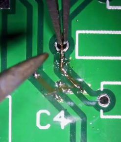
None of this opens the chip package. All of it is real, physical intervention on the board, closer to what “invasive” sounds like in plain English than to what the term means in the strict definition. Speed matters here more than anywhere else in the process: a custom probe fixture or a breakout extension for a connector the design never exposed gets designed and printed on the bench, same day, rather than ordered and waited on. That’s what turns a one-off physical intervention into a repeatable test setup.
Semi-invasive and invasive: die-level, and where the line is drawn
Semi-invasive: package opened (decapsulated), passivation layer intact, no direct electrical contact with the die. Laser and UV fault injection, optical imaging.
Invasive: passivation removed, direct electrical contact with the die itself. Microprobing, FIB circuit edit.
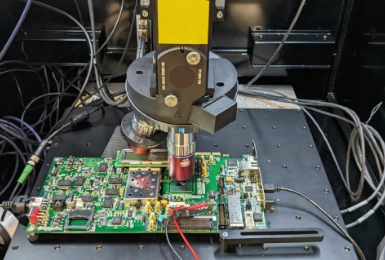
This is out of scope here. Not because the outcome is uninteresting, but because it requires a different equipment class (decapsulation chemistry, FIB) that answers a different question than most embedded products actually need answered. For the large majority of real threat models, the realistic adversary doesn’t have die-level equipment either: a competitor with a teardown budget, a supply-chain actor, an attacker with a bench and a debugger. Board-level access already tells you what that adversary can do. When a threat model genuinely requires die-level work, that’s a different engagement with a different provider, and worth saying plainly rather than quietly stretching scope to cover it.
When to use which
Non-invasive alone: when the unit has to stay intact. Certified hardware, a production sample that can’t be modified, or the question is specifically about side-channel leakage through the device’s existing interfaces.
Board-level: the default for a real assessment. Any signal on the board is reachable, any connection can be modified, faults can be injected directly at the target rather than hoping the external interface responds. The board itself usually survives and goes back together; a potted enclosure, once opened, doesn’t. That cost is worth planning for upfront, not discovering mid-engagement.
Die-level referral: rare, and only when the threat model specifically demands it. Scoped and flagged rather than absorbed into a board-level engagement that can’t actually deliver it.
If your threat model needs to be tested rather than assumed, get in touch. The first step is a short, qualified discovery call.